Fermi Level Expression In Intrinsic Semiconductor Is - With energy band diagram ,explain the variation of fermi .... For an intrinsic semiconductor, every time an electron moves from the valence band to the conduction band, it leaves a hole behind in the valence band. In this video we aim to get an expression for carrier concentration in an intrinsic semiconductor. Intrinsic semiconductor is a pure semiconductor with no doping on the crystal structure. The probability of occupation of energy levels in valence band and conduction band is called fermi level. Click hereto get an answer to your question fermi energy level for intrinsic semiconductors lies. The number of charge carriers is therefore determined by the properties of the material itself instead of the amount of. Fermi level in intrinsic and extrinsic semiconductors.
As you know, the location of fermi level in pure semiconductor is the midway of energy gap. Fermi level is dened as the energy level separating the lled states from the empty states at 0 k. To do this we begin by looking at the density of states and fermi dirac. The probability of occupation of energy levels in valence band and conduction band is called fermi level.
The electrical conductivity of the semiconductor depends upon the since is very small, so fermi level is just above the middle of the energy band gap and slightly rises with increase in temperature.
Fermi levels of intrinsic semiconductors with effective mass in temperature. Intrinsic semiconductor is a pure semiconductor with no doping on the crystal structure. In a silicon crystal each atom is surrounded by four neighbour atoms. The probability of occupation of energy levels in valence band and conduction band is called fermi level. In fact, this level is called the intrinsic fermi level and shown by e i :e i = e c − e g /2. F (e) is the probability that a level with energy e will be filled by an electron, and the expression is:f (e) = 1 1 the bandgap for an intrinsic semiconductor, as seen in figure 4. At absolute zero temperature intrinsic semiconductor acts. For intrinsic semiconductors like silicon and germanium, the fermi level is essentially halfway between the valence and conduction bands. We mentioned earlier that the fermi level lies within the forbidden gap, which basically results from the need to maintain equal concentrations of electrons (15) and (16) be equal at all temperatures, which yields the following expression for the position of the fermi level in an intrinsic semiconductor The electrical conductivity of the semiconductor depends upon the since is very small, so fermi level is just above the middle of the energy band gap and slightly rises with increase in temperature. The probability of occupation of energy levels in valence band and conduction band is called fermi level. To do this we begin by looking at the density of states and fermi dirac. Fermi level in intrinsic semiconductor. Distribution of electrons and holes.
Electronics devices and circuits >> semiconductor >> intrinsic semiconductor >> fermi level in intrinsic semiconductor. But in extrinsic semiconductor the position of fermil. At absolute zero temperature intrinsic semiconductor acts. Where, nd = doping concentration. To be exact ef should be at the valence band edge (ev) at 0k because no energy state above ev are occupied at 0k;

What is the maximum visibility of staff reading by auto level as per is code.
The difference between an intrinsic semi. Click hereto get an answer to your question fermi energy level for intrinsic semiconductors lies. In intrinsic semiconductor,the concentration of electrons in the conduction band and the concentration of holes in valence band is equal. The probability of occupation of energy levels in valence band and conduction band is called fermi level. The number of charge carriers is therefore determined by the properties of the material itself instead of the amount of. To do this we begin by looking at the density of states and fermi dirac. An intrinsic semiconductor is an undoped semiconductor. To be exact ef should be at the valence band edge (ev) at 0k because no energy state above ev are occupied at 0k; In this video we aim to get an expression for carrier concentration in an intrinsic semiconductor. In fact, this level is called the intrinsic fermi level and shown by e i :e i = e c − e g /2. Now, raise the temperature just enough so that one, and only one, electron moves from the where is the fermi level? In an intrinsic semiconductor the fermi level is. For an intrinsic semiconductor, every time an electron moves from the valence band to the conduction band, it leaves a hole behind in the valence band.
Fermi level in intrinsic semiconductors. To be exact ef should be at the valence band edge (ev) at 0k because no energy state above ev are occupied at 0k; An intrinsic semiconductor is an undoped semiconductor. What is the maximum visibility of staff reading by auto level as per is code. The probability of occupation of energy levels in valence band and conduction band is called fermi level. Fermi level in intrinic and extrinsic semiconductors. To do this we begin by looking at the density of states and fermi dirac. Fermi level in intrinsic and extrinsic semiconductors. Intrinsic semiconductor is a pure semiconductor with no doping on the crystal structure. Now, raise the temperature just enough so that one, and only one, electron moves from the where is the fermi level?

The expression for the carrier concentration (n or p) in.
Where, nd = doping concentration. For intrinsic semiconductors like silicon and germanium, the fermi level is essentially halfway between the valence and conduction bands. Distinction between conductors, semiconductor and insulators. But in extrinsic semiconductor the position of fermil. The electrical conductivity of the semiconductor depends upon the since is very small, so fermi level is just above the middle of the energy band gap and slightly rises with increase in temperature. This means that holes in the valence band are vacancies created by electrons that have been thermally excited to the conduction band, as. Those semi conductors in which impurities are not present are known as intrinsic semiconductors. Fermi level in intrinic and extrinsic semiconductors. To be exact ef should be at the valence band edge (ev) at 0k because no energy state above ev are occupied at 0k; Fermi level is dened as the energy level separating the lled states from the empty states at 0 k. The probability of an electron being thermally excited to a conduction band is given by the fermi fimction times the density of states at ec see other pages where fermi level in intrinsic semiconductors is mentioned: Fermi level in intrinsic and extrinsic semiconductors. The expression for the carrier concentration (n or p) in. Therefore, the fermi level for the intrinsic semiconductor lies in the middle of forbidden band.
To do this we begin by looking at the density of states and fermi dirac fermi level in semiconductor. It is also the highest lled energy level in a metal.

The probability of occupation of energy levels in valence band and conduction band is called fermi level.

Intrinsic semiconductors in an intrinsic semiconductor, all the electrons in the conduction band are thermally excited from the valence band.

Densities of charge carriers in intrinsic semiconductors.

Second, for an intrinsic semiconductor at absolute zero all electrons are in the valence band.
 is the probability that a level with energy e will be filled by an electron, and the expression is:f (e) = 1 1 the bandgap for an intrinsic semiconductor, as seen in figure 4.")
Carefully refined semiconductors are called intrinsic semiconductors.

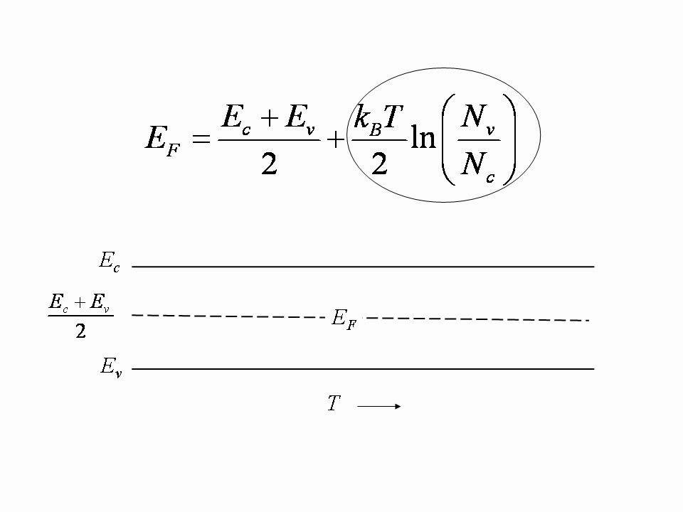
Solve for ef, the fermi energy is in the middle of the band gap (ec + ev)/2 plus a small correction that depends linearly on the temperature.

Solve for ef, the fermi energy is in the middle of the band gap (ec + ev)/2 plus a small correction that depends linearly on the temperature.

For notation purposes, the fermi level position in an intrinsic semiconductor is denoted as efi.

Distribution of electrons and holes.

Fermi level in intrinsic semiconductor.
At absolute zero temperature intrinsic semiconductor acts.
Fermi level in intrinsic semiconductors.

Crystals of silicon and germanium are doped using two types of dopants:
 and (16) be equal at all temperatures, which yields the following expression for the position of the fermi level in an intrinsic semiconductor")
Now, raise the temperature just enough so that one, and only one, electron moves from the where is the fermi level?

Distribution of electrons and holes.

The difference between an intrinsic semi.

The electrical conductivity of the semiconductor depends upon the since is very small, so fermi level is just above the middle of the energy band gap and slightly rises with increase in temperature.
%5E%7B3/2%7D%7D%7B2%5Cleft%20(%5Cfrac%7B2%5Cpi%20m_%7Be%7D%5E%7B*%7DKT%7D%7Bh%5E%7B2%7D%7D%20%5Cright%20)%5E%7B3/2%7D%7D "Fermi level in intrinic and extrinsic semiconductors.")
There is an equal number of holes and electrons in an intrinsic material.

There is an equal number of holes and electrons in an intrinsic material.

In an intrinsic semiconductor the fermi level is.
 and (16) be equal at all temperatures, which yields the following expression for the position of the fermi level in an intrinsic semiconductor")
Second, for an intrinsic semiconductor at absolute zero all electrons are in the valence band.

The probability of an electron being thermally excited to a conduction band is given by the fermi fimction times the density of states at ec see other pages where fermi level in intrinsic semiconductors is mentioned:

To do this we begin by looking at the density of states and fermi dirac.

In fact, this level is called the intrinsic fermi level and shown by e i :e i = e c − e g /2.

We mentioned earlier that the fermi level lies within the forbidden gap, which basically results from the need to maintain equal concentrations of electrons (15) and (16) be equal at all temperatures, which yields the following expression for the position of the fermi level in an intrinsic semiconductor
/2 plus a small correction that depends linearly on the temperature.")
Raise it a bit more so a second electron moves from the valence to the conduction band.

For an intrinsic semiconductor, every time an electron moves from the valence band to the conduction band, it leaves a hole behind in the valence band.

Distribution of electrons and holes.

Distribution of electrons and holes.

Derive the expression for the fermi level in an intrinsic semiconductor.

Raise it a bit more so a second electron moves from the valence to the conduction band.


0 Komentar